Proxmark3 community
Research, development and trades concerning the powerful Proxmark3 device.
Remember; sharing is caring. Bring something back to the community.
"Learn the tools of the trade the hard way." +Fravia
You are not logged in.
Announcement
Time changes and with it the technology
Proxmark3 @ discord
Users of this forum, please be aware that information stored on this site is not private.
#501 2014-03-27 12:07:54
- gaucho
- Contributor
- From: France
- Registered: 2010-06-15
- Posts: 444
- Website
Re: proxmark3 gerbers and bill of material
Hey gaucho
We can get the board even cheaper with parts that cost less. We can change the AT91SAM7S with Cortex M0+, FPGA with cheaper one, 15-20 MSPS ADC.
do they work with the same code?
we have few resources, if we divide on many projects we will not evolve.
Offline
#502 2014-03-27 12:27:14
- Neuer_User
- Contributor
- Registered: 2013-03-26
- Posts: 88
Re: proxmark3 gerbers and bill of material
Concerning kickstarter: The project may not be very innovative, but you would reach more people here. Drawback is that you loose 10% on kickstarter and credit card fees. Bit there have been other RFID-Readers on kickstarter, I remember, so why not?
Offline
#503 2014-03-27 14:03:20
- Enio
- Contributor
- Registered: 2013-09-24
- Posts: 175
Re: proxmark3 gerbers and bill of material
IMHO only two followup projects are feasible.
One making it more accessible (cheap) whilst keeping as much (useful) functionality as possible.
One increasing performance/functionality: (Faster ADC, more bandwith, better FPGA, ARM, maybe external RAM for high frequency, maybe 2 antennas allowing to sync TX/RX on one with snoop on the other, also maybe supporting 848Mhz formats up to analysis into GHz bands).
Offline
#504 2014-03-27 14:38:55
- asper
- Contributor
- Registered: 2008-08-24
- Posts: 1,409
Re: proxmark3 gerbers and bill of material
I an for the 2nd project Enio even if it will be more expensive.
Kickstarter is a great possibility! Many people love hi-tech there!
Offline
#505 2014-03-27 16:06:40
- Enio
- Contributor
- Registered: 2013-09-24
- Posts: 175
Re: proxmark3 gerbers and bill of material
Achieved an improvement:
I managed to stuff 16 bit into the RHR(Receive Hold Register) on ARM where it then is read as a uint16_t (2 samples at once) and stuffed into BigBuffer.
This effectively halves the time consuming read overhead towards that Register and there is enough time to do the check on the RS (Receive Status register) if something has arrived and then read it.
That means now there is no more duplicate samples even on highest possible SSC clock (24Mhz)!
That means we can set the ADC to sample at 13.56 MHz (produces 13.56 MS/s) and effectively read these samples at 3MS/s on ARM. That means we get every 4.52th ADC sample pushed to ARM.
In reality that is we get every 4rth then 5th then 4rth then 5th etc.. So the wave is slightly corrupt on the time line, but the resolution is far better then as if we would sample at 13.56 MHz on SSP (We would get always every 8th sample off adc = 1.695 MS/s)
In the pic in the end you will see that i now have ~28 samples per Bit send from Tag. As we take 3MS/s as base that means we get 28.6 samples per bit, thats why every 2nd bit we see a shift of the grid by ~1 sample.
I will make these 2 sample speeds on SSC optional for the release. It has its use though as you get effectively more information on the wave as with the slower speed.
void optimizedSnoop(void)  // Declared as RAMFUNC in apps.h!
{
  memset(BigBuf, 0, sizeof(BigBuf));
  int n = sizeof(BigBuf) / sizeof(uint16_t);

  uint16_t *dest = (uint16_t *)BigBuf;
  uint16_t *destend = dest + n;

  AT91C_BASE_SSC->SSC_RFMR = SSC_FRAME_MODE_BITS_IN_WORD(16); // Setting Frame mode, 16 bits per word
  // Reading data loop
  while(dest <= destend)
  {
    if(AT91C_BASE_SSC->SSC_SR & AT91C_SSC_RXRDY)
    {
      *dest = (uint16_t)(AT91C_BASE_SSC->SSC_RHR);
      dest = dest + 1;
    }
  }
  //Resetting Frame mode (First set in fpgaloader.c)
	AT91C_BASE_SSC->SSC_RFMR = SSC_FRAME_MODE_BITS_IN_WORD(8) |	AT91C_SSC_MSBF | SSC_FRAME_MODE_WORDS_PER_TRANSFER(0);
}

Last edited by Enio (2014-03-27 16:08:14)
Offline
#506 2014-03-27 16:21:13
- holiman
- Contributor
- Registered: 2013-05-03
- Posts: 566
Re: proxmark3 gerbers and bill of material
Regarding a kickstarter pm3, I'd be interested (and I think a lot more geeks) if it was pm3+. That is: at least decent backwards-compatibility plus more, as mentioned previously. Double antennas, UHF tags etc.
Offline
#507 2014-03-27 16:25:17
- Enio
- Contributor
- Registered: 2013-09-24
- Posts: 175
Re: proxmark3 gerbers and bill of material
Regarding a kickstarter pm3, I'd be interested (and I think a lot more geeks) if it was pm3+. That is: at least decent backwards-compatibility plus more, as mentioned previously. Double antennas, UHF tags etc.
Backwards compatibility.. It would be nice - and we probably rould reuse/integrate alot of the functions, but the whole lower level stuff will have to be reprogrammed mostly from scratch.
Offline
#508 2014-03-27 18:12:38
- gaucho
- Contributor
- From: France
- Registered: 2010-06-15
- Posts: 444
- Website
Re: proxmark3 gerbers and bill of material
Achieved an improvement:
I managed to stuff 16 bit into the RHR(Receive Hold Register) on ARM where it then is read as a uint16_t (2 samples at once) and stuffed into BigBuffer.
This effectively halves the time consuming read overhead towards that Register and there is enough time to do the check on the RS (Receive Status register) if something has arrived and then read it.
That means now there is no more duplicate samples even on highest possible SSC clock (24Mhz)!
...........
This is all really cool. but, why the bits are inverted in the sampled signal? on mifare i usually see the modulation on the bits with logic level 1 and not 0.
Offline
#509 2014-03-27 18:34:31
- gaucho
- Contributor
- From: France
- Registered: 2010-06-15
- Posts: 444
- Website
Re: proxmark3 gerbers and bill of material
I made measurements on not working boards, i was in hurry, and may be i did it wrong.
The hitted command is LF READ if not specified.
These are the results:
-----------------
board1 (blocks and resets hitting lf read): i checked (and compared with working board) the signals SSP, PCK0,SPCK,MISO,MOSI,NCS.
the result is that the SSP_FRAME,SSP_DIN and PCK0 are present, while SSP_DOUT is not present. which is the direction of this signal?who generates it?
SPCK,MISO,MOSI and NCS seems to be ok even if the MOSI doesn't move on the working and on the not working board. Which is the direction of this signal?who generates it?
-----------------------
board2 (LF tune not ok and HF mifare READ not ok). After checking again the soldering, the LF TUNE now it is ok. About the HF read i found that IC10 is not generating the signal on R29. Then, before to say "it is broken" i checked the signal PWR_OE4 (IC10 pin 19). I didn't checked the datasheet but i'm quite sure that this pin is a negated enable signal.
This signal ( PWR_OE4) on the working board is always a logic 1. On the not working board there is a gate, during the HF 14A READ command, where the PWR_OE4 goes to 0.
This causes the board to have less power and, maybe, this causes some problems on the receiving path.
How is it possible that the FPGA moves this signal during HF 14A READ ?
EDIT: what this enable signal is used for? why do we need it? couldn't we just set it to logic 1 all the time?
-------------
i didin't had the time to check the third board.
Last edited by gaucho (2014-03-27 18:41:59)
Offline
#510 2014-03-27 20:39:45
- Enio
- Contributor
- Registered: 2013-09-24
- Posts: 175
Re: proxmark3 gerbers and bill of material
I had the impression via the pwr lines the tx modularion is done. I have time tomorrow evening to check.
Last edited by Enio (2014-03-27 20:40:07)
Offline
#511 2014-03-28 01:03:56
- Enio
- Contributor
- Registered: 2013-09-24
- Posts: 175
Re: proxmark3 gerbers and bill of material
Enio wrote:Achieved an improvement:
I managed to stuff 16 bit into the RHR(Receive Hold Register) on ARM where it then is read as a uint16_t (2 samples at once) and stuffed into BigBuffer.
This effectively halves the time consuming read overhead towards that Register and there is enough time to do the check on the RS (Receive Status register) if something has arrived and then read it.
That means now there is no more duplicate samples even on highest possible SSC clock (24Mhz)!
...........This is all really cool. but, why the bits are inverted in the sampled signal? on mifare i usually see the modulation on the bits with logic level 1 and not 0.
I will compare my cards tomorrow. Thats odd..
Last edited by Enio (2014-03-28 01:05:45)
Offline
#512 2014-03-28 06:20:24
- vivat
- Contributor
- Registered: 2010-10-26
- Posts: 332
Re: proxmark3 gerbers and bill of material
vivat wrote:Hey gaucho
We can get the board even cheaper with parts that cost less. We can change the AT91SAM7S with Cortex M0+, FPGA with cheaper one, 15-20 MSPS ADC.do they work with the same code?
we have few resources, if we divide on many projects we will not evolve.
Cheaper ADC will work without changing the code. Changing the microcontroller and FPGA will require this.
Board 1
I assume that you launched LF READER command. SSP_DOUT is input from ARM to FPGA. But in ./fpga/lo_read.v verilog module it's not used.
Board 2
Try to replace that IC10 tri-state.
Offline
#513 2014-03-28 07:47:59
- Enio
- Contributor
- Registered: 2013-09-24
- Posts: 175
Re: proxmark3 gerbers and bill of material
I checked iso/iec 14443-2 again, iit clearly states:
8.2.5 Bit representation and coding Bit coding shall be Manchester with the following definitions: sequence D the carrier shall be modulated with the subcarrier for the first half (50%) of the bit duration sequence E the carrier shall be modulated with the subcarrier for the second half (50%) of the bit duration sequence F the carrier is not modulated with the subcarrier for one bit duration logical “1” sequence D logical “0” sequence E Start of communication sequence D End of communication sequence F No information no subcarrierNow i am wondering if the phase of the carrier, which we sample at its frequency makes it look different - if adc gets each peak - would it be greater then unmodulated part - and if he always gets low - would it be weaker? Because picc to pcd is just 10% that could be a reason, as its weird that the pcd to picc part is always the same (there its 100% modulation)
Its still not really making sense yet.. pkd sould be enough to smooth it to the peaks of the fc.. ![]()
Edit: Hold on, a 1 starts with modulation in first half. Modulation (active load) means the subcarrier gets weaker(10%) - thats exactly what we get there. I think thenother picture is wrong, my last snoop is right!
Last edited by Enio (2014-03-28 07:57:55)
Offline
#514 2014-03-28 09:04:51
- gaucho
- Contributor
- From: France
- Registered: 2010-06-15
- Posts: 444
- Website
Re: proxmark3 gerbers and bill of material
I checked iso/iec 14443-2 again, iit clearly states:
8.2.5 Bit representation and coding Bit coding shall be Manchester with the following definitions: sequence D the carrier shall be modulated with the subcarrier for the first half (50%) of the bit duration sequence E the carrier shall be modulated with the subcarrier for the second half (50%) of the bit duration sequence F the carrier is not modulated with the subcarrier for one bit duration logical “1” sequence D logical “0” sequence E Start of communication sequence D End of communication sequence F No information no subcarrierNow i am wondering if the phase of the carrier, which we sample at its frequency makes it look different - if adc gets each peak - would it be greater then unmodulated part - and if he always gets low - would it be weaker? Because picc to pcd is just 10% that could be a reason, as its weird that the pcd to picc part is always the same (there its 100% modulation)
Its still not really making sense yet.. pkd sould be enough to smooth it to the peaks of the fc..
Edit: Hold on, a 1 starts with modulation in first half. Modulation (active load) means the subcarrier gets weaker(10%) - thats exactly what we get there. I think thenother picture is wrong, my last snoop is right!
i'm not following you. the filter on hf path suppress the carrier and does a demodulation. a sort of downconversion. the carrier is not available on tp1. this is the reason why you can sample at low frequency and you are not forced to sample at 13/26 MHz or higher. may be i wrote a stupid sentence. take it with care.
what is the tag that you tried? did you tried to upload your first firmware, the one that you uploaded here? i mean: do you exclude it is due to your code?
Offline
#515 2014-03-28 09:19:15
- gaucho
- Contributor
- From: France
- Registered: 2010-06-15
- Posts: 444
- Website
Re: proxmark3 gerbers and bill of material
Board 1
I assume that you launched LF READER command. SSP_DOUT is input from ARM to FPGA. But in ./fpga/lo_read.v verilog module it's not used.
Board 2
Try to replace that IC10 tri-state.
board1: this means that i shall recheck DOUT because i've seen it moving on the working board.
board2: read again my post, IC10 is not transmitting because of the DISABLE pin is activated by the fpga. I will re-measure also this.
Offline
#516 2014-03-28 10:24:02
- Enio
- Contributor
- Registered: 2013-09-24
- Posts: 175
Re: proxmark3 gerbers and bill of material
Edit: Hold on, a 1 starts with modulation in first half. Modulation (active load) means the subcarrier gets weaker(10%) - thats exactly what we get there. I think thenother picture is wrong, my last snoop is right!
i'm not following you. the filter on hf path suppress the carrier and does a demodulation. a sort of downconversion. the carrier is not available on tp1. this is the reason why you can sample at low frequency and you are not forced to sample at 13/26 MHz or higher. may be i wrote a stupid sentence. take it with care.
what is the tag that you tried? did you tried to upload your first firmware, the one that you uploaded here? i mean: do you exclude it is due to your code?
I could not test much yet. I just know - on current code - the test-saw wave i get is as expected. Starts at 0 and goes towards 255, then back to 0. So the sample value and the order should be correct.However i will investigate.
I agree, we basically sample the moving subcarrier, i just meant that from the excerpt of the iso/iec 14443-2 part, the mentioned "modulation on first half of bit" means that the first half of the bit is low, do we agree on this?
Is the PICC->PCD wave correct or not? I think yes.
I will investigate though, regards.
Offline
#517 2014-03-28 18:44:23
- piwi
- Contributor
- Registered: 2013-06-04
- Posts: 704
Re: proxmark3 gerbers and bill of material
I agree, we basically sample the moving subcarrier, i just meant that from the excerpt of the iso/iec 14443-2 part, the mentioned "modulation on first half of bit" means that the first half of the bit is low, do we agree on this?
This is how I understood the ISO14443-2 as well. It even states
Every bit period shall start with a defined phase relation to the subcarrier. The bit period shall start with the loaded state of the subcarrier.
- and therefore implemented it in this way for hf mf sim and hf 14a sim. If Enio's trace is from a simulating PM3 and Gaucho is referring to a real tag then Enio and I obviously misinterpreted the ISO norm (or the card manufacturer did - which is less likely ;-) )
BTW: this thread meanwhile covers several topics - wouldn't it make sense to continue each topic in a separate thread? Maybe then it is read by more people than the group buyers?
Last edited by piwi (2014-03-28 18:47:09)
Offline
#518 2014-03-28 19:01:15
- Enio
- Contributor
- Registered: 2013-09-24
- Posts: 175
Re: proxmark3 gerbers and bill of material
Enio wrote:I agree, we basically sample the moving subcarrier, i just meant that from the excerpt of the iso/iec 14443-2 part, the mentioned "modulation on first half of bit" means that the first half of the bit is low, do we agree on this?
This is how I understood the ISO14443-2 as well. It even states
Every bit period shall start with a defined phase relation to the subcarrier. The bit period shall start with the loaded state of the subcarrier.
- and therefore implemented it in this way for hf mf sim and hf 14a sim. If Enio's trace is from a simulating PM3 and Gaucho is referring to a real tag then Enio and I obviously misinterpreted the ISO norm (or the card manufacturer did - which is less likely ;-) )
I read a bit more about load modulation and indeed, the tag modulates the carrier by producing load in its circuits, that is burning energy taken off the reader's wave - leading to a lower amplitude of the carrier's wave. On my last screen you can even see the frequency of the load/no-load frequency (subcarrier freq is 848khz, thats where the load/no load is happening) in the lows on half of the bits(buffered by the PKD). Im not sure why i had it show the other way around on one of the older snoops, but i guess the since the last snoop is correct (and all i did today are the same) we dont need to find out what went wrong on older code..
BTW: this thread meanwhile covers several topics - wouldn't it make sense to continue each topic in a separate thread? Maybe then it is read by more people than the group buyers?
True, but it more or less evolved out of the primary topic. At some point it would make sense though.
Theres a few things id really like to discuss regarding some design of snoop functionality (my snoop might do lf read as well as hf read with just some option set), but ill put that separate. It might need some changes in how to do the configuration stuff..
Last edited by Enio (2014-03-28 19:02:09)
Offline
#519 2014-03-28 19:16:11
- piwi
- Contributor
- Registered: 2013-06-04
- Posts: 704
Re: proxmark3 gerbers and bill of material
But we should try to find out if the old or the new (FPGA) code is correct. And I would suggest taking a real tag as the reference. How does a snoop look like with a real tag?
Offline
#520 2014-03-28 19:47:26
- Enio
- Contributor
- Registered: 2013-09-24
- Posts: 175
Re: proxmark3 gerbers and bill of material
This last screenshot (http://i.snag.gy/BO0TL.jpg) is a real tag (Mifare 1k). As far as my tests and analyzation goes, the new code is indeed correct. (Tested with sending samples counting in loops from 0-255, i get a perfect saw wave, nothing missing and all values in correct order. And the Mifare wave of last picture looks fine too (ATQA 0x0400).
I want to release it ready for testing asap, but ill need a bit. As there are just 8 major modes for FPGA, and all are taken, well have to find out if we can drop one and keep functionality with mine. That might be a task in itself.. If not we'd have to change the config word to be 16 bits, not 8. I dont know if thats hard to do. It would not hurt at all to have more place for configuration as that way we could set ADC & SSP clock separately (lf/hf snoop in one module) and set carrier separately too (just snoop vs powering the tag and even eventually send stuff -thatll be harder i guess - but for sure doable.).
The ADC->ARM passthru is simple and functional, adding the options and integrating it into the current environment i struggle with..
Last edited by Enio (2014-03-28 19:56:30)
Offline
#521 2014-03-29 11:44:45
- piwi
- Contributor
- Registered: 2013-06-04
- Posts: 704
Re: proxmark3 gerbers and bill of material
You can use one of the minor modes of the iso14443a major mode. They are not all used...
Offline
#522 2014-03-29 14:48:06
- Enio
- Contributor
- Registered: 2013-09-24
- Posts: 175
Re: proxmark3 gerbers and bill of material
You can use one of the minor modes of the iso14443a major mode. They are not all used...
With that amount of options i might need to set for that module, i doubt thats a good idea. We ll see.
Offline
#523 2014-03-31 08:20:59
- vivat
- Contributor
- Registered: 2010-10-26
- Posts: 332
Re: proxmark3 gerbers and bill of material
gaucho
Any news?
Offline
#524 2014-04-01 13:55:14
- gaucho
- Contributor
- From: France
- Registered: 2010-06-15
- Posts: 444
- Website
Re: proxmark3 gerbers and bill of material
BTW: this thread meanwhile covers several topics - wouldn't it make sense to continue each topic in a separate thread? Maybe then it is read by more people than the group buyers?
I agree with you.
@Enio: can you open, if you like to do it, another thread for the new HF sampling feature, and another for the tag modulation?
Write here the new link, if you do it!
@PIWI: for the signal on real mifare 1k tag, you can also watch my oscilloscope screenshot. All the screenshots shows the same result.
@vivat: I was out of office last 5 days, it's an hard period of work.
@Enio: if you upload a working FW i'll try to aquire the signal with my mifare1k, since with your last FW i was not able to see the result of a mifare read command. Maybe because of the wrong delay? can you detail reference firmware used and method?
Maybe there is just a difference in the tag or in the method.
Last edited by gaucho (2014-04-01 13:59:29)
Offline
#525 2014-04-01 15:44:03
- gaucho
- Contributor
- From: France
- Registered: 2010-06-15
- Posts: 444
- Website
Re: proxmark3 gerbers and bill of material
I repeated the measures:
board1:i was partially wrong because on lf read command the board stops and resets after a while and on the SSP_DOUT there is no signal, but on the HF 14A READ command the board does not stops, even if the tag is not read, and the SSP_DOUT moves, so the pin output is not broken.
if this signal is generated by the ARM, as vivat told, i suppose that this signal is not important.
On a working board the SSP_DOUT moves on both commands, but i suppose that, maybe, the arm doens't receive good signal from fpga and for this reason it doesn't reply on this pin.
but why on lf read it doesn't stops and reboots?
what should i check? it seems to me that it's all ok..
board2: i was wrong, because IC10 pin 19 (PWR_OE4) goes HIGH also on a working board, when you hit the HF 14A READ command.
I'm looking for the problem in the wrong place. Generation of the signal is ok.
Offline
#526 2014-04-01 22:36:35
- Enio
- Contributor
- Registered: 2013-09-24
- Posts: 175
Re: proxmark3 gerbers and bill of material
Im very low on time too, sadly - i hope i can get further at the weekend.
Edit: I have plans (after i finish the generic fpga passthru, allowing these hf snoops) to extend it. I want to passthru the data directly to the pc, kind of similar to the circular buffer thing in 14443a part - just with the addition to have a modulation detection included, basically to find the interesting parts. That way we can fill the BigBuffer on ARM with up to 24 Mbit/s (3MS/s) and hand the interesting data over to pc with up to 12Mbit/s (1.5MS/s) with help of usb 1.1. Depending on the size of the gaps between the transmissions, we might be able to snoop the interesting parts of a whole transmission on high detail, not just 40k samples - and if that wont work due to too long transmissions, at least with 13.56 Mhz clock on ssc (13.56 Mbit/s = 1.695 MS/s) it should work out. (We receive on ARM with ~1.7 MS/s and send them over with 1.5 MS/s, the gaps with no modulation should allow to empty the transmit buffer).
This would be really cool imho, im just not exactly sure how to put that into code.
My Idea is to reduce the sample value to be 0x01 to 0xFF (thats -127 to 127 - if adc finds a 0x00 make it 0x01). As i always send 2 samples per frame on ssc we might be able to use 0x00 to mark that a nonmodulated part starts and use the 2nd (or 3rd & 4rth) byte to send the length of the unmodulated part. For example if there is normal samples and then 300 samples not interesting, it would be [0xXX 0xXX ] (last normal sample) [0x00 0xFF](256 boring samples skipped)[0x00 0x2B](44 boring samples skipped) [0xXX 0xXX] (normal samples) - that way we can put it back together on plot to have the sample count (for timing stuff) between modulated data exact. This needs alot of logic in ARM (if theres enough power to not lose samples due to the calculations - i want to test how DMA works for that matter) or in FPGA - or in both.
Ill try to get a thread about all this created coming weekend, however until then, any ideas are welcome here too!
Last edited by Enio (2014-04-01 23:10:46)
Offline
#527 2014-04-02 04:41:07
- vivat
- Contributor
- Registered: 2010-10-26
- Posts: 332
Re: proxmark3 gerbers and bill of material
@vivat: I was out of office last 5 days, it's an hard period of work.
You need to take a rest, or you will make errors in test measurements.
Offline
#528 2014-04-02 08:32:14
- gaucho
- Contributor
- From: France
- Registered: 2010-06-15
- Posts: 444
- Website
Re: proxmark3 gerbers and bill of material
I created a dedicated thread for the new snoop function : http://www.proxmark.org/forum/viewtopic … 573#p10573
check it and continue there.
Last edited by gaucho (2014-04-02 10:21:17)
Offline
#529 2014-04-03 08:52:26
- gaucho
- Contributor
- From: France
- Registered: 2010-06-15
- Posts: 444
- Website
Re: proxmark3 gerbers and bill of material
Yesterday I found another lab in my factory. They suggested to me that there are a lod of cold soldering on the broken boards.
They suggested to place the board on a heated floor at 100°C, then to apply flux to make uniform the temperature on the soldering area, then to solder it again with a welder at 300°. (ok, this is actually what i understood and what i did, not exactly what they told me).
I also found that they have a washing machine and a oven able to automatically resolder entirely the board with a cycle.
If i will not solve by myself, i'll try the oven.
Anyway, now I have the following situation:
Board3: now it works very well.
Board1: HF path is ok, i can successfully read a mifare 1k all the times without error. LF path is not ok, because, as soon as i hit the command LF READ the board stops and after a while it resets. Any ideas? What changes between the 2 commands?
Board2: LF path is ok, i can read and see the plot with the square waveform when there is a tag on antenna. HF path is not ok cause i can't read a mifare.
Yesterday I also received the not working board from Benoit. I changed a resistor, the op.amp and i entirely resoldered it on a heated floor, since i found some unsoldered pins on the fpga. Now it works fine on LF path but on HF path there is a wrong C35 capacitor. Today I'll solder it and I'll let you know.
Offline
#530 2014-04-03 11:45:10
- vivat
- Contributor
- Registered: 2010-10-26
- Posts: 332
Re: proxmark3 gerbers and bill of material
Board1: HF path is ok, i can successfully read a mifare 1k all the times without error. LF path is not ok, because, as soon as i hit the command LF READ the board stops and after a while it resets. Any ideas? What changes between the 2 commands?
Board2: LF path is ok, i can read and see the plot with the square waveform when there is a tag on antenna. HF path is not ok cause i can't read a mifare.
Board1: Can you reflash it with last firmware? Have you tested other LF functions, such as LF HID FSKDEMOD? Did you test the mux/relay?
Board2: Are you sure that tri-states are OK? I already told you to try replacing it.
Offline
#531 2014-04-03 12:26:55
- gaucho
- Contributor
- From: France
- Registered: 2010-06-15
- Posts: 444
- Website
Re: proxmark3 gerbers and bill of material
I replaced the C35 on Benoit's board and now it works correctly.
Finally I have 2 not working boards.
Let's focus on the "macro" problem of Board1: it blocks on lf read command.
I tried some other commands:
command "hw setmux lopkd" doesn't block the board, i also tried the other 3 options of this command successfully
command "hw setlfdivisor" works correctly
command "hw tune" works correctly also with lf antenna
command "hw readmem 10" works correctly
command "lf flexdemod" doesn't block the board
command "lf simbidir" doesn't block the board
command "lf sim" doesn't block the board
command "lf hid clone 20042ea608" works fine and it's actuated correctly (i also checked the result on a working board)
command "lf hid fskdemod" causes the board to block and reset
command "lf read" causes the board to block and reset
command "lf t55 readblock 0" causes the board to block and reset
command "hf 14a read" works correctly by reading mifare tag.
come on, let's find the differences..
p.s.:on this board there is the Enio's fullimage firmware, then this is the latest revision.
Last edited by gaucho (2014-04-03 12:28:35)
Offline
#532 2014-04-03 12:51:23
- holiman
- Contributor
- Registered: 2013-05-03
- Posts: 566
Re: proxmark3 gerbers and bill of material
command "lf hid fskdemod" causes the board to block and reset
command "lf read" causes the board to block and reset
command "lf t55 readblock 0" causes the board to block and reset
In one of the later commits on github, i did some work om 'lf hid fskdemod', I don't know what version you use. The basic operations performed, which are affected by low-level components are not so many. You could try to add a dummy function which calls this, and see where it crashes
void testLFHidLowlevelOperations(int divisor)
{
	DbpString("A");
	FpgaSendCommand(FPGA_CMD_SET_DIVISOR, 95); //125Khz
	DbpString("B");
	FpgaWriteConfWord(FPGA_MAJOR_MODE_LF_READER);
	DbpString("C");

	// Connect the A/D to the peak-detected low-frequency path.
	SetAdcMuxFor(GPIO_MUXSEL_LOPKD);
	DbpString("D");

	// Give it a bit of time for the resonant antenna to settle.
	SpinDelay(50);

	DbpString("E");
	// Now set up the SSC to get the ADC samples that are now streaming at us.
	FpgaSetupSsc();
	DbpString("F");

	if (AT91C_BASE_SSC->SSC_SR & AT91C_SSC_TXRDY) {
		DbpString("G");

		AT91C_BASE_SSC->SSC_THR = 0x43;
		LED_D_ON();
	}
        DbpString("H");
	if (AT91C_BASE_SSC->SSC_SR & AT91C_SSC_RXRDY) {
		DbpString("I");
		dest[i] = (uint8_t)AT91C_BASE_SSC->SSC_RHR;
		i++;
		LED_D_OFF();
		}
        DbpString("J");

}
Offline
#533 2014-04-03 13:04:42
- Enio
- Contributor
- Registered: 2013-09-24
- Posts: 175
Re: proxmark3 gerbers and bill of material
The reason it blocks might be that it doesnt get data off ssc - In main loop if the function arm checks for data on ssc in a while loop - while(bigbuff is not full) check for incoming data and put in BigBuf.
I cant check now - How is ssc clocked on lf? How is adc_d clocked? Does pck0 arrive at fpga(it comes from arm)?
Because asc_d on hf is clocked by 1356mht clock, on lf its pck0/divisor.
Offline
#534 2014-04-03 14:35:40
- gaucho
- Contributor
- From: France
- Registered: 2010-06-15
- Posts: 444
- Website
Re: proxmark3 gerbers and bill of material
@enio: ok, i'll check these signals and i'll post a feedback.
@holiman: this is a kind of debug i was looking for. unfortunately i don't have the environment to compile the FW and i never did it. It is possible that i loose time tring to do this stuff. Ofcourse i have to learn cause i want to write my finctions, but i wish first to solve these problems on these boards and send them all to the owners.
Last edited by gaucho (2014-04-03 14:36:06)
Offline
#535 2014-04-03 16:32:55
- gaucho
- Contributor
- From: France
- Registered: 2010-06-15
- Posts: 444
- Website
Re: proxmark3 gerbers and bill of material
board1 is kidding with me.
since HF commands were working and LF READ was blocking the board, i decided to aquire signals on HF 14A READ command and then to compare them with LF READ command signals. But while doing this aquisitions, the board stopped to work also on HF 14A READ command.
Now I don't know what to think: it resets also on HF 14A READ (HW tune and HW setlfdivisor are working without reset)
Anyway, since i aquired some signals while HF 14A READ command was working, i decided to compare these measures with the same measures performed now that the board no more works on HF 14A READ command.
This is the result:
PCK0 (hf 14a read working)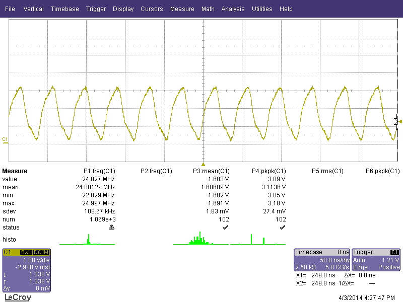
PCK0 (hf 14a read resetting board)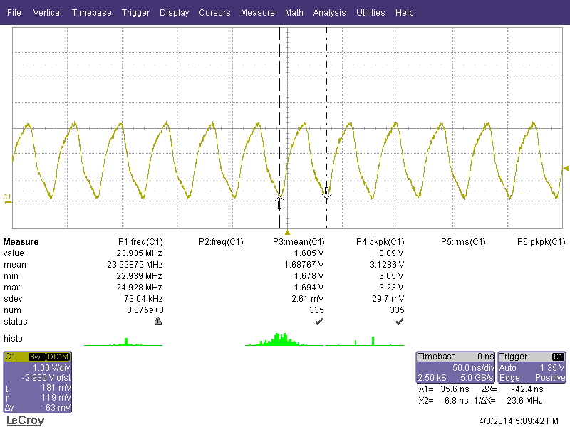
SPCK (hf 14a read working)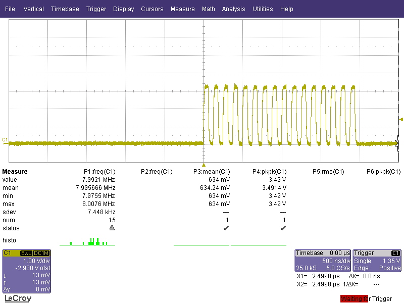
SPCK (hf 14a read resetting board)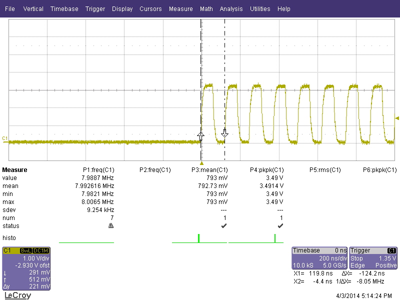
SSP_CLK (hf 14a read working)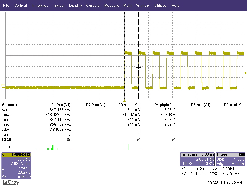
SSP_CLK (hf 14a read resetting board)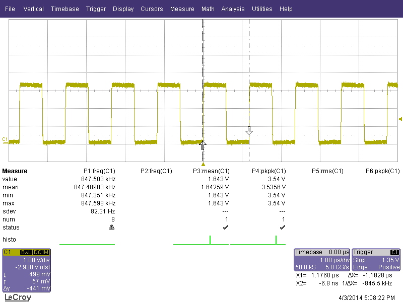
ADC_CLK (hf 14a read working)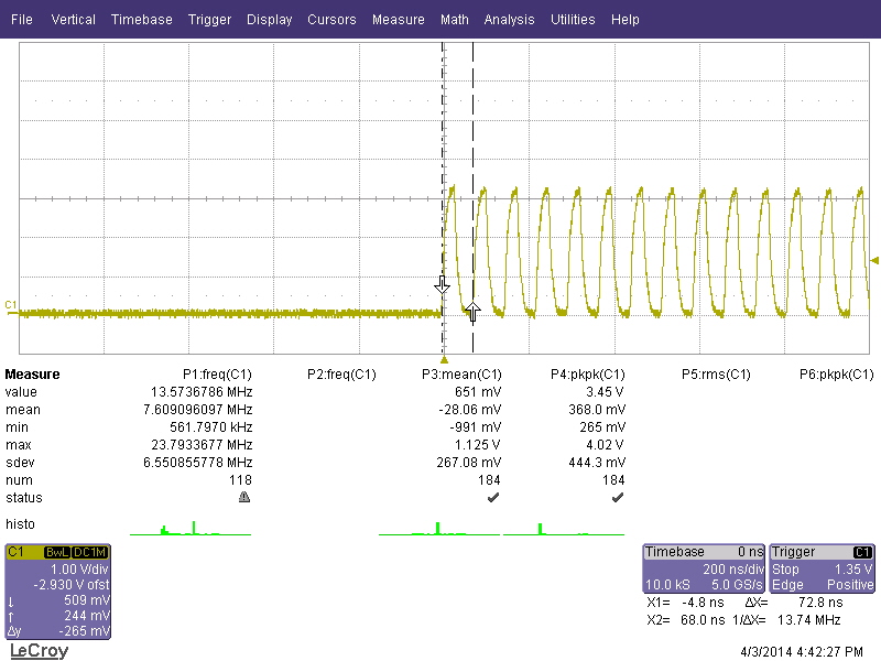
ADC_CLK (hf 14a read resetting board)
SUMMARY: there is no difference in these signals between when the board was working and when the board was resetting.
Offline
#536 2014-04-03 16:45:37
- Enio
- Contributor
- Registered: 2013-09-24
- Posts: 175
Re: proxmark3 gerbers and bill of material
Could try a debugprint if or what comes thru ssc. Maybe also addfew more dbgprints to observe where it dies. I can help you at weekend with that.
Offline
#537 2014-04-04 04:02:40
- vivat
- Contributor
- Registered: 2010-10-26
- Posts: 332
Re: proxmark3 gerbers and bill of material
gaucho
Do you hear the relay click when you plug it into USB?
IMHO The problem is in analog RX path or relay/mux.
I think you have incorrectly performed mux test. You should do this:
1. hw setmux lopkd
2. check with multimeter continuity test between relay pin 4
3. repeat for other 3 modes
Another test is to compare oscilloscope screenshots from TP1.
Offline
#538 2014-04-04 07:51:52
- gaucho
- Contributor
- From: France
- Registered: 2010-06-15
- Posts: 444
- Website
Re: proxmark3 gerbers and bill of material
@vivat: ok, i will do it, but a missing command actuation(mux) is not blocking the arm.
the fpga should appy the setting(set mux), aquire the signal and send it back to the arm. The only check it should be made on the serial communication between fpga and arm. Since the connections are good, i suspect a damaged arm or fpga.
Does someone of you knows better the sequence of operations on the serial line?
How to guess the broken component between the 2?
@Enio: If you could help me i will appreciate cause you still made some modifications on the code and it will be easy for you, you'll be faster than me.
Last edited by gaucho (2014-04-04 07:52:35)
Offline
#539 2014-04-04 10:48:40
- vivat
- Contributor
- Registered: 2010-10-26
- Posts: 332
Re: proxmark3 gerbers and bill of material
the fpga should appy the setting(set mux)
ARM sets the mux, not FPGA.
aquire the signal and send it back to the arm. The only check it should be made on the serial communication between fpga and arm. Since the connections are good, i suspect a damaged arm or fpga.
Maybe you are correct, but if you have broken ARM, it wouldn't respond to ANY command and if you have bad FPGA, it wouldn't read HF tags and write to LF...
Does someone of you knows better the sequence of operations on the serial line?
How to guess the broken component between the 2?
Do you mean SSC? For which command?
Offline
#540 2014-04-04 14:07:40
- gaucho
- Contributor
- From: France
- Registered: 2010-06-15
- Posts: 444
- Website
Re: proxmark3 gerbers and bill of material
Do you mean SSC? For which command?
"hf14a read" in example
or "lf read", if you prefer.
Maybe you are correct, but if you have broken ARM, it wouldn't respond to ANY command and if you have bad FPGA, it wouldn't read HF tags and write to LF...
I think you could also have a situation where only a part of the ARM/FPGA could be damaged(not the entire chip).
I have only a spare fpga (not the arm) but i want to better think about its replacement since i paid it 8€ (excluded shipping cost) and it takes to me at least one hour for soldering.
Last edited by gaucho (2014-04-04 14:14:29)
Offline
#541 2014-04-04 20:27:06
- holiman
- Contributor
- Registered: 2013-05-03
- Posts: 566
Re: proxmark3 gerbers and bill of material
Gaucho,
If you want to do a modification, it's really easy.
You can use an already existing command, let's say you pick 'lf ti read'. In armsrc/appmain.c, you can check what method that usb-command gets dispatched to:
		case CMD_READ_TI_TYPE:
			ReadTItag();
			break;
Most (all?) lf-operations are in lfops.c. That's where you'll find ReadTItag, around line 136:
void ReadTItag(void)
{
	// some hardcoded initial params
	// when we read a TI tag we sample the zerocross line at 2Mhz
	// TI tags modulate a 1 as 16 cycles of 123.2Khz
	// TI tags modulate a 0 as 16 cycles of 134.2Khz
	#define FSAMPLE 2000000
	#define FREQLO 123200
	#define FREQHI 134200

	signed char *dest = (signed char *)BigBuf;
	int n = sizeof(BigBuf);
//	int *dest = GraphBuffer;
//	int n = GraphTraceLen;
[...]
So, let's just hijack that one :
void testLFHidLowlevelOperations()
{
	DbpString("A");
	FpgaSendCommand(FPGA_CMD_SET_DIVISOR, 95); //125Khz
	DbpString("B");
	FpgaWriteConfWord(FPGA_MAJOR_MODE_LF_READER);
	DbpString("C");

	// Connect the A/D to the peak-detected low-frequency path.
	SetAdcMuxFor(GPIO_MUXSEL_LOPKD);
	DbpString("D");

	// Give it a bit of time for the resonant antenna to settle.
	SpinDelay(50);

	DbpString("E");
	// Now set up the SSC to get the ADC samples that are now streaming at us.
	FpgaSetupSsc();
	DbpString("F");

	if (AT91C_BASE_SSC->SSC_SR & AT91C_SSC_TXRDY) {
		DbpString("G");

		AT91C_BASE_SSC->SSC_THR = 0x43;
		LED_D_ON();
	}
        DbpString("H");
	if (AT91C_BASE_SSC->SSC_SR & AT91C_SSC_RXRDY) {
		DbpString("I");
		dest[i] = (uint8_t)AT91C_BASE_SSC->SSC_RHR;
		i++;
		LED_D_OFF();
		}
        DbpString("J");

}
void ReadTItag(void)
{
    testLFHidLowlevelOperations();
}
Compile, flash, then you should be able to invoke the test-method via 'lf ti read'.
Offline
#542 2014-04-04 20:33:26
- Enio
- Contributor
- Registered: 2013-09-24
- Posts: 175
Re: proxmark3 gerbers and bill of material
Compile, flash, then you should be able to invoke the test-method via 'lf ti read'.
I think Gaucho has not set up his pc for compiling, thats what i understood - hes not into this stuff yet - can you compile him a fullimage? As he doesnt need a client update that should go fine.
Offline
#543 2014-04-04 20:43:07
- holiman
- Contributor
- Registered: 2013-05-03
- Posts: 566
Re: proxmark3 gerbers and bill of material
Sure, I'm not connected to my pm3 and in a bit of a rush right now, so I haven't tested it. It's basically the code above (minus some compilation errors) dunked right into the latest github code. Here it is: http://martin.swende.se/fullimage.elf .
Offline
#544 2014-04-04 20:49:57
- Enio
- Contributor
- Registered: 2013-09-24
- Posts: 175
Re: proxmark3 gerbers and bill of material
Cool, if that doesnt work i can do one tomorrow.
Edit: I just checked - the main difference between LF and HF on fpga is - on LF the clock on ssc is pck0 (coming from arm) divided by some divisor to match 125 khz/134khz. On HF the 13.56MHz clock is used, not coming from arm.
I think - on the arm part - we never get a RXREADY in Status register and stay in the loop until after ~15s it resets (happens on my hf snoop too when we dont get a trigger before 15ish s).
Gaucho, you measured pck0 is on the pin from arm - can we be sure the pin on fpga is soldered well? Because if pck0 doesnt arrive at fpga well, it would be natural ssc doesnt get data stuffed into arm and we stay in that loop until reset..
It could also be PLL of which pck0 is derived from but then usb would probably not work because the clock for usb is PLL/2 too (PLL=96MHZ, usb clock 48, pck0 24)
Last edited by Enio (2014-04-04 21:05:12)
Offline
#545 2014-04-04 21:58:28
- holiman
- Contributor
- Registered: 2013-05-03
- Posts: 566
Re: proxmark3 gerbers and bill of material
As I've said earlier in this thread, I appreciate the work you guys are doing ( still hope to get me another pm3), but don't have much to contribute on the low-level electronics. But if there's anything I can do on the programming side, let me know.
Offline
#546 2014-04-06 07:05:39
- vivat
- Contributor
- Registered: 2010-10-26
- Posts: 332
Re: proxmark3 gerbers and bill of material
vivat wrote:Do you mean SSC? For which command?
"hf14a read" in example
or "lf read", if you prefer.
For lf read command FPGA is set to execute lo_read.v module. You can see an example how is data transferred:
// example of ssp transfer of binary value 1100101
// start of transfer is indicated by the rise of the ssp_frame signal
// ssp_din changes on the rising edge of the ssp_clk clock and is clocked into
// the ARM by the falling edge of ssp_clk
//             _______________________________
// ssp_frame__|                               |__
//             _______         ___     ___
// ssp_din  __|       |_______|   |___|   |______
//         _   _   _   _   _   _   _   _   _   _
// ssp_clk  |_| |_| |_| |_| |_| |_| |_| |_| |_| |_

// serialized SSP data is gated by ant_lo to suppress unwanted signal
assign ssp_din = to_arm_shiftreg[7] && !ant_lo;
// SSP clock always runs at 24Mhz
assign ssp_clk = pck0;
// SSP frame is gated by ant_lo and goes high when pck_divider=8..15
assign ssp_frame = (pck_divider[7:3] == 5'd1) && !ant_lo;
As I already said, you can check pins 31, 32, 34, 71 of FPGA(SSP_FRAME, SSP_DIN, SSP_DOUT, SSP_CLK) with logic analyzer and running some command, like lf read.
Offline
#547 2014-04-06 08:06:47
- gaucho
- Contributor
- From: France
- Registered: 2010-06-15
- Posts: 444
- Website
Re: proxmark3 gerbers and bill of material
Sure, I'm not connected to my pm3 and in a bit of a rush right now, so I haven't tested it. It's basically the code above (minus some compilation errors) dunked right into the latest github code. Here it is: http://martin.swende.se/fullimage.elf .
thank you holiman, enio is correct, i have no problem to understand and modify the code, it's just that i still have not downloaded and setup the environment for compile. i don' t know how much time i need to do it. i 'll use your code.
Offline
#548 2014-04-06 08:11:16
- gaucho
- Contributor
- From: France
- Registered: 2010-06-15
- Posts: 444
- Website
Re: proxmark3 gerbers and bill of material
Cool, if that doesnt work i can do one tomorrow.
Edit: I just checked - the main difference between LF and HF on fpga is - on LF the clock on ssc is pck0 (coming from arm) divided by some divisor to match 125 khz/134khz. On HF the 13.56MHz clock is used, not coming from arm.
I think - on the arm part - we never get a RXREADY in Status register and stay in the loop until after ~15s it resets (happens on my hf snoop too when we dont get a trigger before 15ish s).Gaucho, you measured pck0 is on the pin from arm - can we be sure the pin on fpga is soldered well? Because if pck0 doesnt arrive at fpga well, it would be natural ssc doesnt get data stuffed into arm and we stay in that loop until reset..
It could also be PLL of which pck0 is derived from but then usb would probably not work because the clock for usb is PLL/2 too (PLL=96MHZ, usb clock 48, pck0 24)
interesting. thanks for analisys.
pck0 was measured on fpga pin.
Offline
#549 2014-04-06 08:19:16
- gaucho
- Contributor
- From: France
- Registered: 2010-06-15
- Posts: 444
- Website
Re: proxmark3 gerbers and bill of material
As I've said earlier in this thread, I appreciate the work you guys are doing ( still hope to get me another pm3), but don't have much to contribute on the low-level electronics. But if there's anything I can do on the programming side, let me know.
I will continue to try. when we will all together decide that it's time for me to stop tring the repair, we can divide the cost of these 2 broken boards and 2 person can get back the money and the other guys can receive their working board. It's 180€ divided by 20.
Then i can start manufacturing my GauchoPM3 since i decided to order by myself quantity1 PCB and to solder by myself components and check if my 2 layers board project works.
But i will not complete the pcb design until i don't finish the repairing.
p.s.: i convinced my chief to buy a 3d printer, within 4 months i will design a pm3 ABS case.
Last edited by gaucho (2014-04-06 08:28:34)
Offline
#550 2014-04-06 16:30:06
- gaucho
- Contributor
- From: France
- Registered: 2010-06-15
- Posts: 444
- Website
Re: proxmark3 gerbers and bill of material
i forgot to add 8%, for paypal fees, to the 180€
Offline